
Wolfspeed Now Sells a Higher-Grade 200 mm SiC Wafer, Aiming to Lift Chip Yields
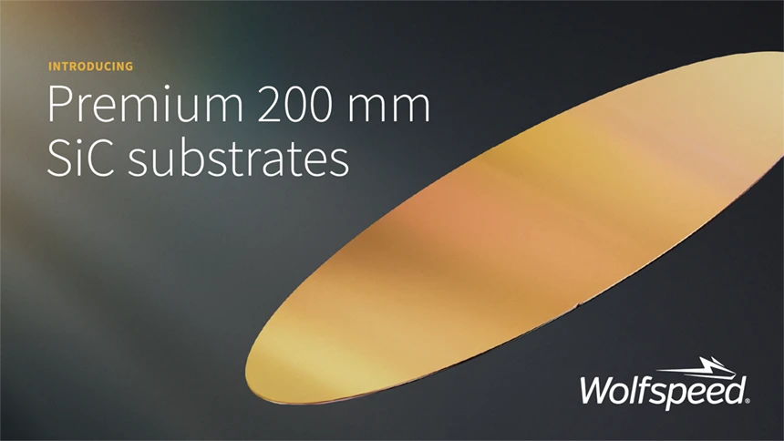
Wolfspeed has begun selling a premium-grade 200 mm n-type silicon carbide substrate, a starting material the company says is meant to help chipmakers get more working devices out of every wafer. The new offering slots into a 200 mm SiC materials family that Wolfspeed first put on the commercial market in September 2025.
The pitch centers on defect control. Wolfspeed reports fewer than 0.01 micropipes per square centimeter in the new substrate — equating to fewer than three across an entire wafer — a figure it says was confirmed through X-ray topography, the inspection method the company regards as the industry standard. Wolfspeed also calls its threading screw dislocation count low, though it did not disclose a specific number.
Why does that matter? A micropipe is a hollow-core screw dislocation that cuts through the SiC crystal and then extends up into the epitaxial layer grown on top. When a device happens to sit above one, it tends to break down under high voltage. Because the likelihood of a die overlapping a defect grows with die size, defect density in the substrate has an outsized effect on yield for large, high-current chips — exactly the devices drawing the most interest from EV power electronics designers.
Wolfspeed argues that cleaner bare wafers, paired with tighter wafer-shape control and lot-to-lot consistency, translate into better epitaxial results using customers’ existing processes. Reducing variability in the starting material, the company says, improves the chances of getting a design right the first time and shortens qualification timelines. The company is accepting orders, and says it has set aside dedicated capacity, maintains a product expansion roadmap and can add new capacity within its current SiC manufacturing site. Cengiz Balkas, Executive Vice President of Wolfspeed’s Materials Business Unit, framed the launch as giving customers “a stronger foundation for developing increasingly demanding silicon carbide devices, backed by the manufacturing experience and scale to support them as needs grow.”
What do you think?